B. SOMANATHAN NAIR
In this article, we present a
physical model that will help to understand the behavior of a transistor
amplifier in the common-emitter configuration. In the CE configuration, a small
base current (in the microampere range) is controlling a much larger collector
current (in the milliampere range). How can a small current induce control over
a much larger current? To answer this, we use the following model.
Figure 1 shows a model in which we
have two interconnected paths. One path is narrow through which only one electron
can move. Let this represent the base-emitter path. Similarly, let the second
path, which represents the collector-emitter path, be much larger and can
permit three electrons to move through it.
Let electron E1 move around the
base-emitter path and let electrons E2, E3, and E4 move around the
collector-emitter path. The four electrons share the common path between base
and emitter. It can be seen that it is in this region that E1 interacts with E2,
E3, and E4. The question here is how do they interact?
The answer to this lies in the fact that there exists
a tiny magnetic field surrounding every electron (i.e., electron is a tiny magnet).
When base electron E1 meets collector electrons E2, E3, and E4 in the common (base-emitter)
path, their magnetic fields interact with each other. When a signal voltage is applied
to E1, the magnetic field surrounding it will vary (i.e., get modulated) according
to the variations in the signal. These variations in the magnetic field around E1
will induce similar variations in the magnetic fields of E2, E3, and E4 while
they traverse through the common path. This theory can be extended to the
actual case where millions of electrons are involved.
Thus the variations in the tiny input base current
due to the signal input voltage induce corresponding variations in the larger
collector current by the interaction of magnetic fields surrounding individual
electrons. This in turn produces amplification of the signal in the
common-emitter. Figures 2, 3, and 4 illustrate the relevant operations further.
Figure 2 shows the situation when the electrons are
injected from the emitter region under the action of supply voltages VBB and VCC and input
signal voltage Vs. It is in this region that the magnetic
fields around the electrons start interacting with each other. The signal
variations created in the base electron gets transferred to the collector
electrons creating corresponding variations in the collector current. Since
there are millions of electrons In the base current and millions and millions of
electrons in the collector current, we find that signal variations in a very
low-value base current is able to create corresponding variations in the much
larger collector current, producing amplification, as stated above.

Figure 3 shows the situation when the base electron
and collector electrons enter the base region. Here also interaction of
respective magnetic fields occurs.
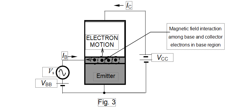
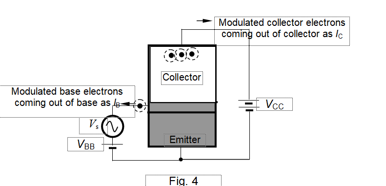
Figure 4 shows the condition when the modulated
base electron comes out of the base and the modulated collector electrons come
out of the collector. It can be seen that the collector current carries the
larger variation (modulation) in it resulting in amplification of signal
voltage as stated earlier.


No comments:
Post a Comment