Saturday, 21 April 2018

BLOCK DIAGRAM REDUCTION IN CONTROL SYSTEMS - A SIMPLE ALGEBRAIC METHOD


B. SOMANATHAN NAIR
P. S. CHANDRAMOHANAN NAIR


ABSTRACT

In this paper, we present a very simple and straightforward method for reducing complex-looking block diagrams. The main advantage of this method is that the last step in the reduction process directly gives the expression of the transfer function of the system. The reduction process requires only an introductory knowledge of elementary algebra.


1. INTRODUCTION

         Currently two methods are described in the Control-System literature1,2,3,4 for reducing complex-looking block diagrams. These are, respectively, the ‘Mason’s gain formula’ and the ‘moving-block method’.

            Mason’s gain formula1,2,3 suffers from the following drawbacks:

·       It becomes difficult in some cases to identify all the feed-forward and feed-back paths.

·    In several cases, it may become difficult to identify all the closed loops in the system. It is interesting to note that the number of closed loops in Problem 3.14 of Reference 1 is actually 4; but it was miscalculated as 3 loops in the Reference 2 (this was corrected in Reference 1). This proves our argument.

·     It is difficult for a beginner to identify all the touching and non-touching loops in the system.

·      Identification of co-factors is difficult in many situations.

The difficulties mentioned above will lead to a wrong derivation of the control ratio of the system.

           The second method known as 'moving-block (or summing-point)' method1,2 is also a complicated operation. The problems associated with this method are the following:

·        It is difficult to remember several expressions related to the moving of a block in the forward direction and in the reverse direction past a summing point.

·     For each such movement, one has to redraw the new block-diagram configuration.

·    Unless the above operations are carefully done, this method can also lead to wrong answers.

            The method described in this paper involves no previous knowledge of any complex formulas and requires only an elementary knowledge of algebra. The method is simple, straightforward and can be applied easily.

2. A NEW SIMPLE ALGEBRAIC METHOD

The first step in the new method is to identify and name all the nodes in the block as E1,  E2, etc., where E’s represent respective error signals. Once the nodes are named, we start writing simple algebraic equation for each node that gives the value of the E signal of that node. The method can be best illustrated by explaining an actual example.

Example 1: Figure 1 shows the block diagram to be reduced and Fig. 2 shows the same block diagram with the respective nodes designated.

            In Fig. 2, we find that there are six nodes, designated as E1, E2, E3, E4,  E5, and E6, respectively. Of these six, we immediately recognize that node 

E5 = C


            We now proceed to write the algebraic equation for each of the nodes. Thus at Node 1, we find
           
                                                         E1 = R ‒ C                                          (1)

At Node 2, the equation becomes
                                     
                                                       E2 = E1 + E5 H1                                    (2)

Now, in our method, we immediately substitute for E1 from Eq. (1) into Eq. (2). Thus
                                   
                                                   E2 = R ‒ C + E5H1                                    (3)

At Node 3, the equation is
   
                                                                 E3 = G1H2                                   (4)

We now substitute for E2 from Eq. (3) into Eq. (4). Thus
                                   
        E3 = G1(R ‒ C + E5H1)
                                                = G1R ‒ G1C + E5G1H1       (5)

Now, the equation at Node 4 is

                                           E4 = E3 ‒ C H2                                 (6)
                                                                                         

Substituting for E3 from Eq. (5) into Eq. (6) yields
                       
                              E4 = G1R ‒ G1C + E5G1H1 ‒ C H2                                         (7)

Next we have the equation for Node 5 as

                                                   E5 = E4G                                   (8)

Now, substituting for E4 from Eq. (7) into Eq. (8), we get

                               E5 = (G1R ‒ G1C + E5G1H1 ‒ C H2)G2                                                               
   =G1G2R‒G1G2C+E5G1G2H1‒CG2                              (9)

Rearranging Eq. (9), we obtain

                                                E5(1‒G1G2H1)=G1G2R‒G1G2C‒CG2H2      (10)

from which we get

         E5=G1G2R‒G1G2C‒CG2H2 /(1‒G1G2H1)          (11)

Finally at the output node, we find

                                            C = E6 = E5G3                                                             (12)

Substituting for E5 from Eq. (11) into Eq. (12), and simplifying after manipulations, we get the control ratio


In the method described above, we have used the technique of substituting for each of the E functions from its previous equation. Thus equation for E2 is obtained by substituting the expression for E1, equation for E3 is obtained by substituting the expression for E2, and so on, until we reach the expression for C. This reduces the complexity of solving for all the equations simultaneously in the end, and greatly simplifies the solution. As can be seen from the procedure, the solution of the last equation yields the control ratio C/R directly.

Example 2: Figure 3 shows the block diagram of a system slightly more complex than the one shown in Fig. 1. In this case also, we proceed in the same manner as was done in the case of Example 1.

            In the diagram shown in Fig. 3, we first mark all the E (error) nodes. In this case we find that there are seven nodes. We also find that Node E7 is output node C itself.


We now proceed to write the algebraic equation for each of the nodes. Thus at Node 1, we find

                                                     E1 = R  ‒ E4 H1                                                               (1)

At Node 2, the equation is
                                               
                                                     E2 = G1 E1                                                                         (2)

Now, we substitute for E1 from Eq. (1) into Eq. (2), which yields
                                                
                                                 E2 = RG1 ‒ E4 G1 H1                                                            (3)

 At Node 3, the relation becomes

                                                  E3 = E2 + E6 H3                                                            (4)

Substituting for E2 from Eq. (3) into Eq. (4) gives

                                       E3 = RG1 ‒ E4 G1 H1     + E6 H3                                                     (5)

The equation for Node 4 can be written as
                                                    
E4 = E3 G2 = RG1 G2 ‒ E4 G1 G2 H1   + E6 G2 H3                             (6)

where we have used Eq. (5). Rearranging Eq. (6), we get

                                                   E4(1‒ G1 G2 H1) =  RG1 G2  + E6 G2 H3                       (7)


From Eq. (7), we find
    
                                                E4=  (RG1 G2 + E6 G2 H3 )  /(1‒ G1 G2 H1)                       (8)

The equation for Node 5 is given by

E5  = E4‒ CH2  = (RG1 G2 + E6 G2 H3 )  /(1‒ G1 G2 H1) ‒ CH2                               (9)

where we have substituted for E4 from Eq. (8) to yield E5. Now, equation for Node 6 is

                                                      E6 = G3E                                                                 (10)

Substituting for E5 from Eq. (9) into Eq. (10) gives the expression
                 
                                       
            E6 =  (RG1 G2 + E6 G2 H3 )G/(1‒ G1 G2 H1) ‒ G3CH2                          (11)

Rearranging Eq. (11), we have

                       
            E6 (1(H3G2G3)/(1 + G1G2 H1 )
                                   = RG1G2 G3/[(1 + G1G                                             (12)                              


At Node 7, the output C can now be written as

                                                            C = E7 = E6 G4                                                            ­(14)

Substituting for E6 from Eq. (13) into Eq. (14), we obtain

Rearranging Eq. (15), we find

From Eq. (16), we get the control ratio as


Example 3: Figure 4 shows a two-input control system. We have to obtain the control ratios C/R and C/D of this system.
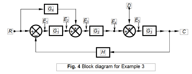


As in the above cases, we start with Node 1. With respect to Node 1, we find


                                                            R ‒ CH = E1                                                                   ­(1)

At Node 2, we have
           
E2 = G1E1 = (R ‒ CH)G1                                                                (2)


Now, with respect to Node 3, we obtain

E3 = E2+ G4R = (G1+G4)R ‒ CHG1                                            (3)

At Node 4, we find

                       
E4 = E3G2 = (G1+G4)R G2 ‒ CHG1G2                                                  (4)


And at Node 5,

                                    E5 = E4 ­+ D = (G1+G4)R G2 ‒ CHG1G2 +D                                  (5)


Finally, at Node 6,

C= G3 E5 = (G1+G4)R G2G3 ‒ CHG1G2 G+D G3                                                 (6)

Rearranging Eq. (6) yields the value of C [see  Eq. (7) below]


                                                                                                                                    (7)
            
To find C/R, we must assume D = 0. Then from Eq. (7), we obtain


 Similarly, to find C/R, we must assume R = 0. Then from Eq. (7), we obtain


3. CONCLUSION

We have demonstrated here a very simple and easy method for finding the control ratio of complex block diagrams representing control-system installations. It assumes no previous knowledge of finding feed-forward or feed-back paths and other complex computations involved in the usage of Mason’s gain formula nor does it require the remembrance of any complicated block-moving formulas. All it requires is the usage of simple algebra to solve the basic equation associated with each node of the system in a systematic and step-by-step fashion.

4. REFERENCES

  1. Katsuhiko Ogata, Modern Control Engineering, 3rd ed, Prentice-Hall, 1990
  2. Katsuhiko Ogata, Modern Control Engineering, 2rd ed, Prentice-Hall, 1997
  3. Norman S. Nise,  Control Systems Engineering, 6th ed., Wiley India, 2011
  4. C. Mei, On Teaching the Simplification of Block Diagrams, Int. J. of Engng. Ed, (Great Britain) Vol. 18, No. 6, pp 697-703, 2002.


At Node 7, the output C can now be written as 


Tuesday, 17 April 2018

COMMON-EMITER AMPLIFIER MODEL TO EXPLAIN WORKING PRINCIPLES


B. SOMANATHAN NAIR

            In this article, we present a physical model that will help to understand the behavior of a transistor amplifier in the common-emitter configuration. In the CE configuration, a small base current (in the microampere range) is controlling a much larger collector current (in the milliampere range). How can a small current induce control over a much larger current? To answer this, we use the following model.
            Figure 1 shows a model in which we have two interconnected paths. One path is narrow through which only one electron can move. Let this represent the base-emitter path. Similarly, let the second path, which represents the collector-emitter path, be much larger and can permit three electrons to move through it.
            Let electron E1 move around the base-emitter path and let electrons E2, E3, and E4 move around the collector-emitter path. The four electrons share the common path between base and emitter. It can be seen that it is in this region that E1 interacts with E2, E3, and E4. The question here is how do they interact?


The answer to this lies in the fact that there exists a tiny magnetic field surrounding every electron (i.e., electron is a tiny magnet). When base electron E1 meets collector electrons E2, E3, and E4 in the common (base-emitter) path, their magnetic fields interact with each other. When a signal voltage is applied to E1, the magnetic field surrounding it will vary (i.e., get modulated) according to the variations in the signal. These variations in the magnetic field around E1 will induce similar variations in the magnetic fields of E2, E3, and E4 while they traverse through the common path. This theory can be extended to the actual case where millions of electrons are involved.
Thus the variations in the tiny input base current due to the signal input voltage induce corresponding variations in the larger collector current by the interaction of magnetic fields surrounding individual electrons. This in turn produces amplification of the signal in the common-emitter. Figures 2, 3, and 4 illustrate the relevant operations further.

Figure 2 shows the situation when the electrons are injected from the emitter region under the action of supply voltages V­BB and VCC and input signal voltage Vs. It is in this region that the magnetic fields around the electrons start interacting with each other. The signal variations created in the base electron gets transferred to the collector electrons creating corresponding variations in the collector current. Since there are millions of electrons In the base current and millions and millions of electrons in the collector current, we find that signal variations in a very low-value base current is able to create corresponding variations in the much larger collector current, producing amplification, as stated above.
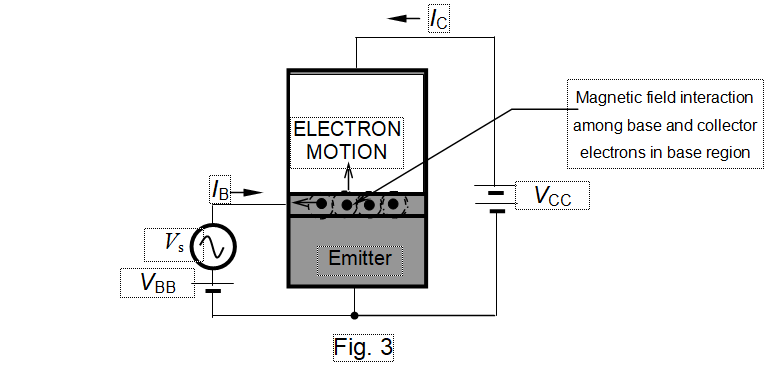
Figure 3 shows the situation when the base electron and collector electrons enter the base region. Here also interaction of respective magnetic fields occurs.

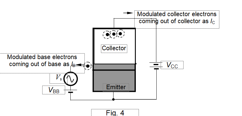
Figure 4 shows the condition when the modulated base electron comes out of the base and the modulated collector electrons come out of the collector. It can be seen that the collector current carries the larger variation (modulation) in it resulting in amplification of signal voltage as stated earlier.


Sunday, 15 April 2018

COMMON-BASE CONFIGURATION STUDY OF OUTPUT CHARACTERISTICS USING HYDRAULIC MODEL


B. SOMANATHAN NAIR

Figure 1 shows the common-base (CB) configuration of a PNP-type bipolar junction transistor with its emitter-base junction forward biased (FB) and collector-base junction reverse biased (RB). It can be seen that, under these biasing conditions, emitter current IE flows through the base to the collector. It can also be seen that the emitter current gets divided as collector current IC and base current IB. Since the base is very narrow, we find that IB is much smaller than IC and that Iis almost equal to IE.


The operation of CB configuration can be studied using Fig. 2, which shows a hydraulic model of the CB configuration. In this model, we have a driving pump in the first pipe section and a suction pump in the third pipe section. The driving pump is similar to the forward bias in the emitter-base region and suction pump is similar to the reverse bias in the collector-base region.   
The driving pump drives current from the first pipe section (equivalent to the emitter current IE through the emitter) into the second and third pipe sections. A major portion of this current (i.e., IE) flows to the third pipe section (i.e., collector region) as collector current IC, which will be sucked away by the suction pump (i.e., acting similar to the reverse bias between collector and base). A small portion of the current (i.e., emitter current) flows through the narrow middle pipe section (i.e., base region) as the base current IB. It can be seen that
I­E = I­C + I­B

Now, if IE varies, then IC varies in the same fashion. Thus the changes in the input current are regenerated in the output current as such and hence the CB configuration can act as an amplifier.


It can be seen that current flows through the collector even if the suction pump is removed. This operation is similar to the CB configuration with VCC removed (Fig. 3). We thus find that I flows even when VCC= 0. This is because even though VCC= 0 (by shorting the collector-base terminals), the path is completed for the emitter-supply voltage VEE, which will drive the emitter current through the collector. Thus we find that IC is almost equal to Ieven when VCC = VCB = 0 (here we use the notation VCB to indicate the voltage between collector and base terminals since in plotting characteristics, we use terminal voltages rather than supply voltages). This is clearly indicated in the characteristic (Fig. 5).


Now, to make IC = 0, we have to convert the suction pump (reverse bias) into a driving pump (forward bias). Then collector current will flow from collector into base so that IC = IE. Since the two currents oppose each other, the net collector current will become zero. This is shown in Fig. 4. Figure 5 shows one CB output characteristic.


In Fig. 5, we find that I­C becomes zero at about V­CB = 0.8 V. It may also be noted that the curve for +V­CB resembles that of a forward-biased (C-B) diode. This condition is usually called saturation. Thus, when both the junctions are forward biased, we get the saturation condition of the transistor amplifier. It may be noted that since VCC (or VCB) = VEE (or VEB) for saturation condition, the net voltage VCEsat (VCBVEB) = 0, ideally. However, since E-B junction is heavily doped and C-B junction is lightly doped, usually VCEsat = 0.1 to 0.2 V.


AMPLIFICATION

B. SOMANATHAN NAIR
     
      When we hear the word amplification, we get the feeling that a small quantity of an item is made into a much larger quantity of that item by using a specially made instrument called amplifier. For example, an audio amplifier amplifies low-volume sound signals into a high-volume sound signal. But, there is one problem for this definition: it is against the law of conservation of energy. According to this law, a small quantity of energy can not be converted into a large quantity of energy; one form of energy can be converted into another form only without any change in its magnitude. Then what is amplification?

AMPLIFICATION (IDEAL DEFINITION)

Amplification is the process of controlling the flow of energy, the controlling energy being negligibly smaller than the controlled energy.

ILLUSTRATIVE EXAMPLE 1

The ideal definition says that amplification is the control of flow of energy. In this ideal definition, we do not find any word that has any relation to the word amplification. Then how can we say that this is the definition of amplification?   
            Let us consider a procession in which there is one leader and five followers as shown in Fig. 1. The leader shouts a slogan and his followers repeat the same in the same way the leader has shouted. The combined voice of the five followers gives an amplified version of the leader’s voice by a factor of five. In other words, we say that in this operation, we get amplification by a factor of five.

 The following points are important in this context:

1.       There is one input voice.

2.       There are five output voices.

3.     The input voice is able to control the output voices. For example, if the input says, “Jai Sriram”, all the outputs will say, “Jai Sriram”. Now, if the input says, “Jai, Jai, Jai Sriram”, the outputs will also say, “Jai, Jai, Jai Sriram”. Thus the outputs follow the variations in the input exactly in the same fashion, but at a much larger volume. Hence, we say that the system consisting of one leader and five followers has produced an amplification of five.

4.  In this case, the law of conservation of energy is not violated, i.e., we are not generating a large energy from a small energy. Both small (i.e., leader) and large (five followers) energies exist; only, the small energy is controlling the large energy in such a way that the variations in the small (controlling) energy are reproduced exactly in the same fashion in the large (controlled) energy. Incidentally, we find that this is the ideal definition of amplification (i.e., small energy controlling large energy).

5.    It may be noted that the controlling and controlled energies are both DC energies (i.e., there are no variations in them).

6.     We super impose the signal to be amplified to the controlling energy and apply it to the input section of the amplifying device.

7.   The amplifying device then produces variations in the larger energy in its output section corresponding to the variations in the input energy. The larger output, which reproduces the input variations exactly as such, then gives amplification.


ILLUSTRATIVE EXAMPLE 2      


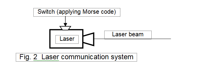
Consider a laser torch emitting 1 milliwatt of red laser light (Fig. 2). Let this light be used for communication between a man on ship and a man on the shore. First assume that the shoreman sends laser light to the shipman. A steady laser light is a DC signal and has no meaning. To send information, we must use variations in the DC light, which are known as codes.

        There several coding schemes that we use. In this case, let us assume that Morse code is used, which makes use 1s and 0s for information transmission. 1s may be represented by presence of a short light pulse while its absence may be used to represent 0 (or vice versa). The laser light can be switched on or off by a small switch on the outer cover of the laser; a slight pressure on the switch will turn on or off the laser light.
Now suppose the shoreman wants to send certain information to the ship. He will prepare the Morse code of the information first and then press the laser switch as per the codes formed. The pressing of the laser key requires negligible power. Thus the power input is very small and this creates the signal input energy. But this input energy creates corresponding variations in the large laser energy so that the shipman can read the message by decoding the variations in the light energy. In this case, we see that amplification has occurred, since the input energy (pressing of the laser switch) is small, but the output energy (laser light) is large.          

ILLUSTRATIVE EXAMPLE 3


Consider now a common-emitter electronic amplifier. In this case, input current is the base current (microampere range) and output current is the collector current (milliampere range). Since 1 mA is 1000 μA, amplification is possible in this case. This is because the small variations in the base current can create corresponding variations on a lager scale in the collector current (for further explanation on CE amplification, see the forthcoming blog on CE amplification).


Friday, 6 April 2018

WHY DO WE NEED DIRECT CURRENT IN COMMUNICATION?


B. SOMANATHAN NAIR

We require multiple-level current or voltages for signal representation. The minimum number of levels that we require for this purpose is two and we call this as the binary system. Direct current has only one level and hence it cannot be used to represent signals. But we find that DC currents and voltages find extensive application in electronics and communications. For example, most of the electronic devices require DC voltages for their operation.
            A course in electronic circuit theory usually starts with the theory of half-wave and full-wave rectifiers. But usually no descriptions are seen about the importance of DC current and rectifiers in the electronic circuit textbooks that a student generally follows. The following illustrative examples will highlight the importance of DC in communication.

ILLUSTRATIVE EXAMPLE 1

Consider the case of human conversation. Let one man talk to another man. Here the preposition to shows the direction of flow of human voice energy. Once the direction of energy flow is fixed, then we no longer use the word to show the direction of signal flow. It can also be seen that to represents one direction and hence constitutes a DC signal, which means that in a conversation, DC is used to indicate direction. Without this unidirectional energy flow we can not communicate with each other. But once we get the direction of sound energy flow, we no longer care for this DC component.

ILLUSTRATIVE EXAMPLE 2

Let us now take the case of human vision. Consider a room in which some objects are kept. We see these objects when a steady (DC) light (such as a tube light) is present. Here the light acts as the DC part and the objects act as signals. Once we start to see objects we no longer are bothered about the DC light source. However, we are bothered about the light source when it becomes off and we can not see the objects even though they are still there in the room.  Thus DC light acts as the background which help us to see objects. It may be noted that it is difficult to see objects when the steady DC light is replaced with a variable light source, whose intensity varies at every instant.  

ILLUSTRATIVE EXAMPLE 3

Consider a white board (or computer screen) for writing. A white board may be considered as a DC surface, because it carries a steady whiteness on its surface. Now let us write something on the surface. The white background now carries signal on it. Without the background surface, we can not write anything on it. Thus DC acts as the background in this case. Once the idea is written on the board, we no longer care for the background board unless it becomes too shady that we can not write anything further on it.  

ILLUSTRATIVE EXAMPLE 4

Consider the traffic through road, rail, sea etc. suppose we concentrate on road traffic using a car. Car takes a person from one destination to another. Since this is a directional movement, we can say that the car is a DC source. The person is the signal. The car (DC) carries the signal (person) from one destination to another. Once this transportation is over, we no longer need the car and neglect this DC component.

ILLUSTRATIVE EXAMPLE 5

Consider now a common-emitter amplifier. In this amplifier, we forward bias the base-emitter region with about 0.65 volt DC, and reverse bias (indirectly) the collector-emitter region with 10 volt DC. These DC voltages are required to make the base and collector currents, respectively. Now, the signal to be amplified is superimposed above the input base current. Thus the base current is a variable DC (DC bias current + ac signal current). This variable DC current produces corresponding variable and amplified DC collector current. However, once we get the amplified collector signal current, we remove the DC component part in it by using a coupling capacitor and get the amplified signal current across the collector-emitter output terminals. It can be seen that the DC currents are used in this case also to give specific directions to the flow of collector and base currents. Once this is established, we discard the DC.

CONCLUSION

We have seen that DC is essential in every communication system. It shows direction of energy flow or background needed to support the signal. Without DC there is no communication. This is the reason why it is included in the electronic circuit theory syllabus.

Tuesday, 3 April 2018

HOW MUCH SECRECY IS THERE IN OUR ONLINE DATA TRANSMISSION?

B. SOMANATHAN NAIR

Currently, in India, a lot of discussions are going on regarding the safety of digital data transmitted through internet. Let us analyze the situation and see how safe our digital data are from intruders.
Suppose we sent an email to a friend. This involves the following operations. First we prepare the letter by typing it on our personal computer. Next we turn on our internet connection and access our email by using our email ID and password. After these operations, we access the email of the friend to whom the letter must be sent, and send the letter either directly or as an attachment. It can be seen that this is a simple procedure.
As stated above, sending and receiving emails is a simple procedure. We feel that because of the password protection, nobody else, except the sending and receiving parties of the email, can read the data sent over internet. This would have been true if the data were sent by enclosing it in a sealed cover. However, there is no cover in email transactions and hence there is no secrecy of data.
It is well known that all mail transactions are controlled by server computers, which are owned by the mail company. The data we sent over mail will be first stored in these server memories, from where they will be transferred to the recipient of the mail. These operations show that all the data transferred through email are stored in the server memories of the email company and hence are not secret. The email company can access these data anytime they want.
Elaborating the discussions given above, we find that any data sent over internet are stored in the memories of the internet providing company and hence are not secret documents. This means that all online transactions are done with the knowledge of the internet provider; he will have access to all types of information that are transmitted through online. This point suggests that there are no data on internet that are private and hence secret.
The above point stresses one thing: Any data stored on the internet server memories can be read and viewed by the internet provider without any difficulty. However, it may be noted that these data can be viewed by hackers also. Hackers are people who illegally intrude into networks to steal data that are stored there. Password-security is not a problem for such people. There are several expert software engineers all over the world who work as expert hackers. No security measures are a problem for such people. They are expert crackers who steal into various networks and access data stored therein.
            Now, consider the claims that data stored in personal identification cards of a person are safe by various authorities of government. From the arguments given above, we can see that these claims are thoroughly false. It is clear that all the information regarding a person stored in his personal identification card is known to the internet service provider and hacking experts. Hence, it is astonishing to know that some service providers are summoned by various governments to explain the leakage of personal data.
            In this context, it is surprising to note that some educational organizations send question papers and answer papers online to agencies who conduct the examinations. It is not surprising to hear that the question papers have leaked.
            Similarly, in election polls using voting machines, manipulations are possible. Expert hackers in IT field can manipulate the results of the election.
            It is further interesting to note that nothing is a secret now-a-days in this world. We believe that what we are doing inside the four walls of our room is totally invisible to any outside person. This idea is also wrong. There are several satellites sent by various governments and agencies orbiting around the earth. Some of these satellites are designed as spy satellites, which can snoop into the private life of persons. These satellites carry very powerful cameras working on infrared frequencies. They are so sensitive that they can snoop into the rooms of houses and take the images of activities taking place in these rooms. Since the frequency involved is infrared, the affected parties will have no knowledge about the photoshoot from the satellite. This idea is alarming; however it is a reality now. Thus the phrase ‘privacy of persons’ no longer exists. This means that we have no privacy in our life. Governments and corporates decide our fate.

DISCRETE SIGNAL OPERATIONS

EDITOR: B. SOMANATHAN NAIR 1. INTRODUCTION In the previous two blogs, we had discussed operations of scaling and shifting on conti...